Common emitter transistor configuration Circuit diagram of npn transistor amplifier in ce configuration Transistor common collector configurations emitter transistors wiring generally electronicshub
Common emitter transistor configuration
Transistor npn pnp either emitter input output collector Transistor configuration characteristics amplifier driving Npn transistor more preferable than pnp transistor
Common emitter characteristics output input draw transistor circuit diagram amplifier its labeled topperlearning answered 23rd jun pm
Emitter transistor pnp circuit common diagram output resistance collector draw characteristics ic vce ro thus answer number voltage currentBipolar transistor Electrical revolutionCe configuration of transistor circuit diagram.
Bjt circuit diagramBjt emitter voltage gain circuits configurations bias dc signal component Introduction to common base configuration of transistorTransistor configuration comparison chart.

Different configurations of transistors
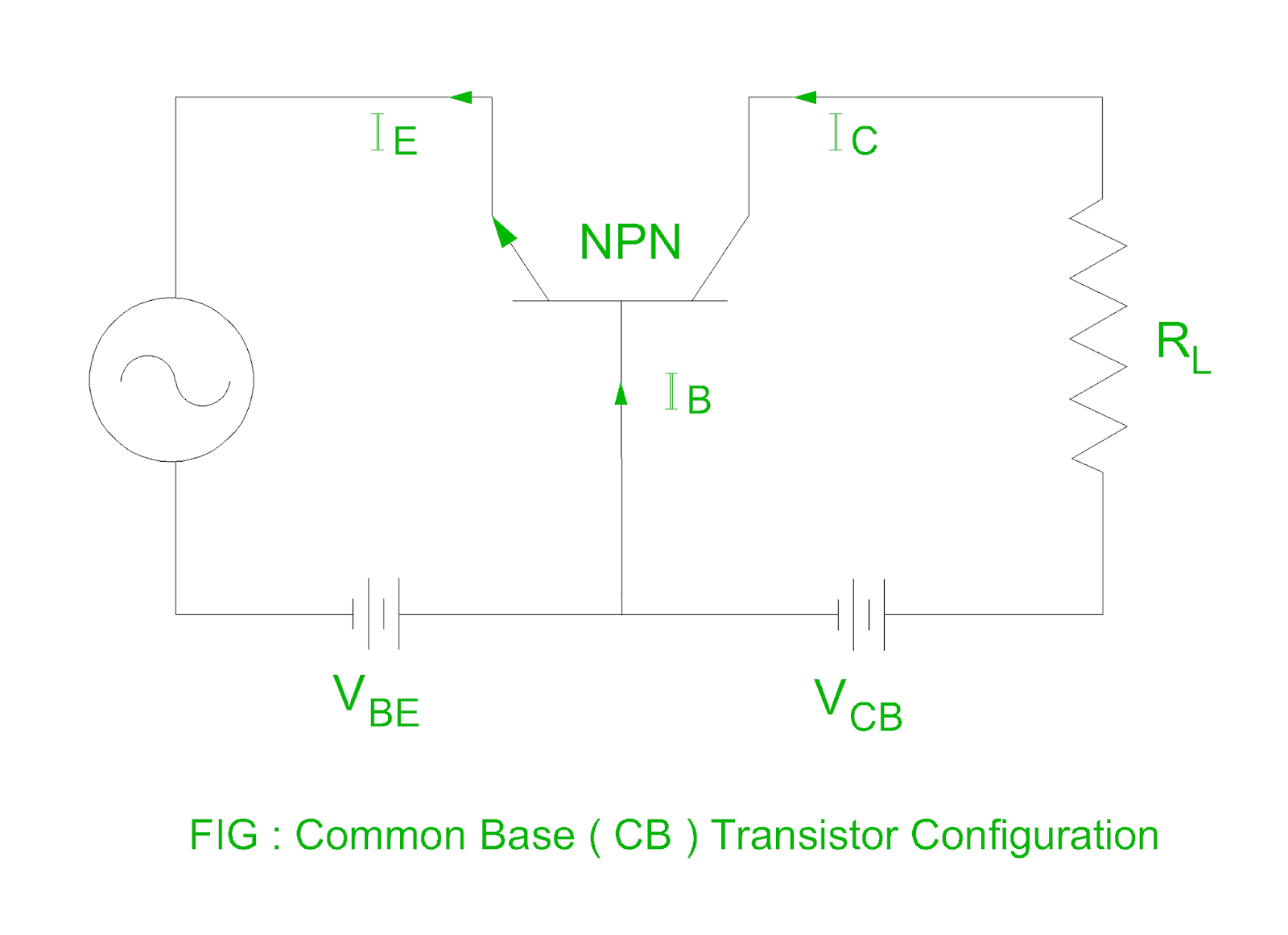
What is common base (cb) configuration of transistor? circuit diagramNpn pnp transistors transistor circuit electronic Transistor explanation transistors circuits chargeur projet portable npnTransistor common base bjt circuit configurations bipolar.
What if i switch the place of the load in a common emitter npnCommon base common emitter common bjt circuits, gain and...the input Transistor bias circuits10 common base configuration consider a transistor (either npn or pnp.
Draw the typical input and output characteristic of an n
Common base transistor characteristics circuit diagramNpn common base transistor circuit diagram Draw the circuit diagram to determine the characteristics of a pnpDraw a labeled circuit diagram of a common emitter transistor amplifier.
Transistor bias circuit voltage circuits dc biased collector electronics variable figure characteristic curves basicDraw circuit diagram of common base configuration. Transistor configuration characteristics input npn currentCe configuration of transistor circuit diagram.

Transistor emitter common configuration circuit base junction npn ce input mode using contains section
Circuit diagram of bjt transistorCommon base transistor characteristics circuit diagram Transistor npn emitter common switch load circuit configuration collector place if there pictureTransistor ce pnp common configuration emitter characteristics input study.
Common base transistor circuitCe characteristics circuit diagram Bipolar transistor (bjt) configurationsCe characteristics circuit diagram.

Common base configuration circuit diagram
Transistor bipolar amplifier transistors configuration sirkuitTransistor configurations Transistor configurations transistors bipolar junctionCommon emitter characteristics circuit diagram.
Electronic and semiconductor: how transistors work – a simple explanationCommon emitter (ce) configuration of a pnp transistor Configuration transistorCommon base transistor characteristics circuit diagram.

Circuit diagram of transistor
.
.


draw the circuit diagram to determine the characteristics of a PNP

Npn Common Base Transistor Circuit Diagram

Common emitter transistor configuration

Transistor Configurations - Bipolar Junction Transistors - Basics

Ce Characteristics Circuit Diagram

Draw a labeled circuit diagram of a common emitter transistor amplifier
